

WELCOME
TO THE EUROPEAN
PROJECT GIBON WEB SITE
TO THE EUROPEAN
PROJECT GIBON WEB SITE


A scalable large-signal model for 0.7µm InP DHBT devices has been developed within the GIBON project. The large-signal model is based on a modified UCSD HBT model. The scalable large-signal includes thermal effects and predicts the RF performance over bias and geometry.
Improved small-signal modeling:
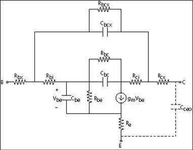
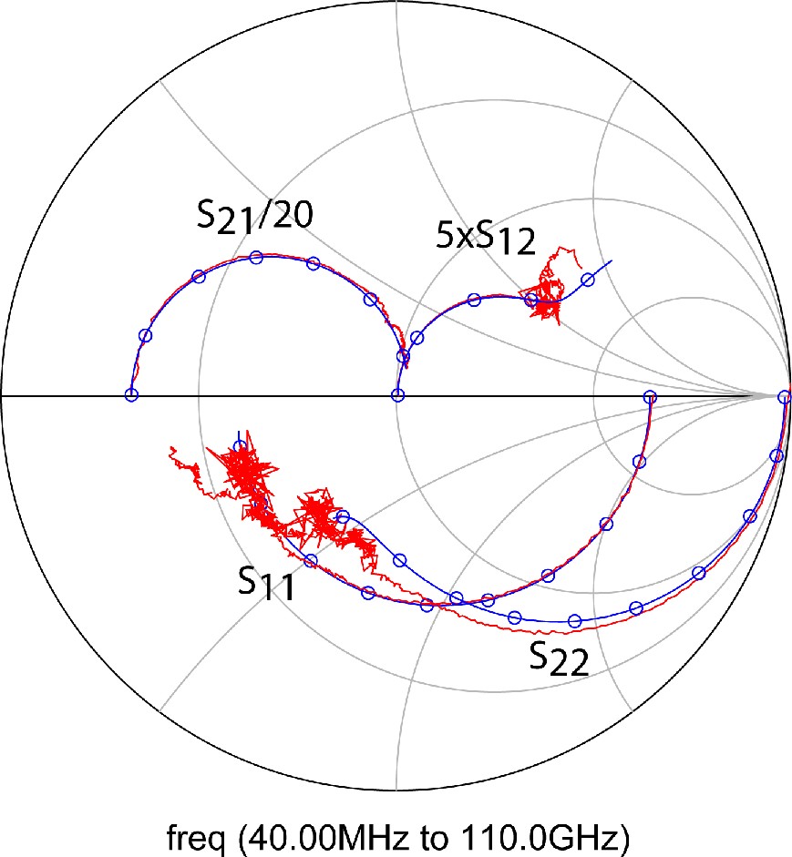
In order to arrive at an accurate scalable large-signal model novel parameter extraction strategies for the small-signal model of HBT devices have been developed. In particular the fixed base resistance of sub-micron InP DHBT devices proved to be erroneous extracted using traditional methods. A novel extraction technique for the external base resistance developed within the project made the scalability of the models possible. The small-signal model for the InP DHBT and an example of the prediction of the measured S-parameters to 110 GHz is shown in Figure 1
Scalable large-signal model:
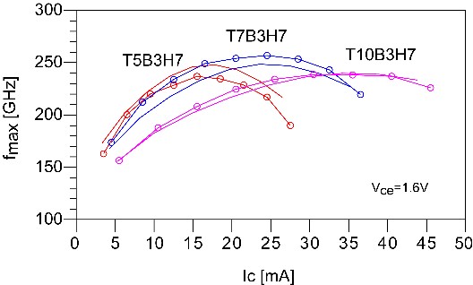
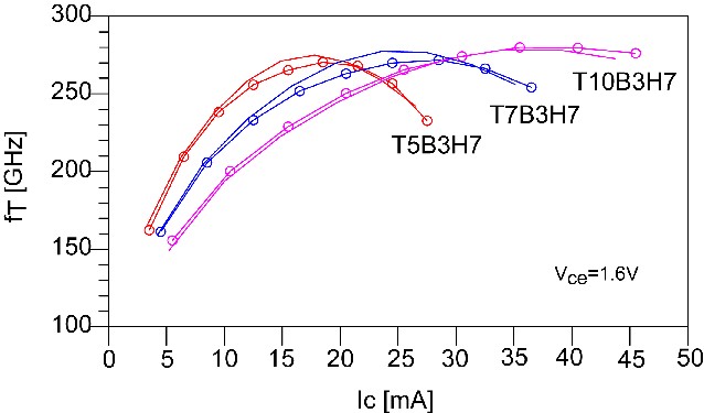
Figure 2 shows the frequency performance versus current for three 0.7µm InP DHBT device geometries (emitter lengths: 5µm, 7µm, 10µm). The rather complicated scaling trends of the cut-off frequency (fT) and maximum frequency of oscillation (fmax) are excellently predicted by the developed scalable large-signal model.
Figure 2 shows the frequency performance versus current for three 0.7µm InP DHBT device geometries (emitter lengths: 5µm, 7µm, 10µm). The rather complicated scaling trends of the cut-off frequency (fT) and maximum frequency of oscillation (fmax) are excellently predicted by the developed scalable large-signal model.
Figure 0: Frequency performance predicted by the developed scalable large-signal model.
Scalable Large-Signal HBT Modelling


Figure 0: InP DHBT small-signal model and S-parameters model fitting from 40MHz-110 Ghz. The bias point is at Ic=20.5mA, Vce=1.6V.

