


WELCOME
TO THE EUROPEAN
PROJECT GIBON WEB SITE
TO THE EUROPEAN
PROJECT GIBON WEB SITE


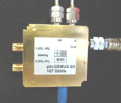
By combining a high-speed photodiode and a Decision Flip-Flop in a same package, a high sensitivity demultiplexing receiver was reported at last Optical Fiber Conference (San Diego, March 22-26, 2009). The InP-based 1.55 mm high-speed photodiode is of the waveguide-integrated type exceeding 105 GHz bandwidth. The demultiplexing circuit is a Decision Flip-Flop fabricated in the InP Double Heterojunction Bipolar process (0.7 µm emitter width, 270 GHz cut-off frequency). Co-packaging the two devices in a same module greatly reduces electrical losses due to separate housings and interconnections by roughly 6 dB. Consequently world-leading sensitivities can be obtained.
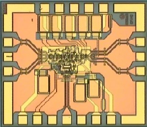
Micrograph of the Decision Flip-Flop (left); eye diagrams of an input electrical signal at 100 Gbit/s and associated output tributary at 50 Gbit/s (right)
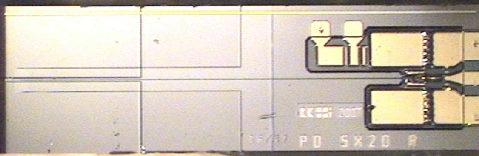
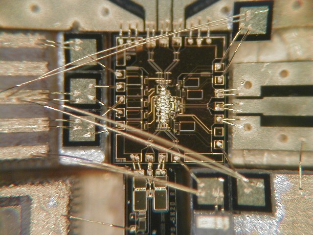
Micrograph of the waveguide-integrated photodiode (left); intimate copackaging within one module housing by connecting the detector chip and the DEMUX chip with ultrashort bonding wires (right)
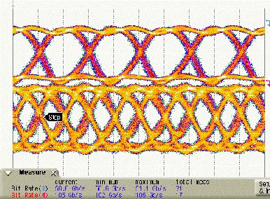
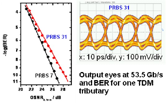
With a 107 Gbit/s, RZ-OOK input optical signal, the co-packaged photoreceiver allows recovery of the tributaries, without any error floor for the longer sequences, illustrating the good performance of the devices and the quality of the integration technology
GIBON 100 Gbit/s demultiplexing receiver: a first innovative module