


WELCOME
TO THE EUROPEAN
PROJECT GIBON WEB SITE
TO THE EUROPEAN
PROJECT GIBON WEB SITE


Electro-Absorption Modulated Lasers (EML) belong to the Photonic Integrated Circuits family: they integrate a DFB laser with an electro-absorption modulator. The EML developed in GIBON is characterized by specific features:
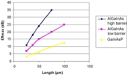
- An AlGaInAs QW material structure with enhanced electro-absorption effect and high modulation efficiency. Such a structure allows designing an efficient modulator in spite of a limited length: 12 dB for a 50 µm long modulator, with a DC efficiency of 6 dB/V.
- A Semi-Insulating Buried Heterostructure (SI-BH) structure with good optical properties (low optical loss) and suitable for large bandwidth applications owing to the low excess capacitance and low series resistance.
- Single active layer for both the laser and modulator active sections, for simple processing.
- The overall EML bandwidth goes up to 60 GHz, suitable for the 100 Gbit/s objectives. Ways to improve this bandwidth (reduced capacitance while keeping a constant resistance) have been identified.
Extinction ratio as a function of EAM length (10 QW, tensile strain), illustrating the superiority of the AlGaInAs system efficiency.
WP2 Transmitter integration (Lead partner: ATL)
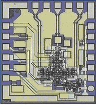
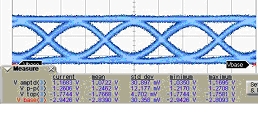
Microphotograph of the selector-driver chip. Input data and clock are coming from the pads at the top; the output signal is generated at the pad in the lower right, to ease the EML pigtailing. The eye diagram above is measured at 86 Gbit/s
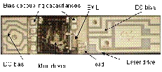
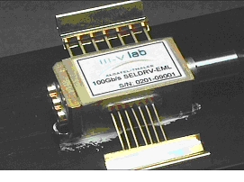
Carrier with interconnected driver, EML and load resistance (above). On the right is the completed module with the 3 input connectors and output fiber pigtail.
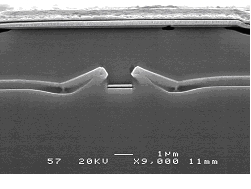
Scanning Electron Microscopy image of a SI-BH waveguide cross-section
InP Heterojunction Bipolar Transistors are well suited for the design of high-speed mixed-signal circuits. A processing technology (self-aligned, triple mesa structure, on 3 SI InP substrate) was developed in the early phase of GIBON, with an emitter width of 0.7 µm. HBTs were demonstrated, characterized by cut-off frequencies in the 270-300 GHz range (Fmax and Ft respectively), and breakdown voltage of 4V. Several types of circuits were then designed and fabricated:
- Amplifiers specifically designed as EML drivers, providing a 1V output swing voltage with an output offset of -2.5 V.
- Driver amplifiers with larger output voltage. With the lumped amplifier design, output voltage is > 2V, with a maximum differential output voltage reaching > 2x2V using the two complementary outputs.
- Selector and Flip-Flop ICs were also designed and fabricated for the MUX and DEMUX needs. Good operation of these circuits was checked at 107 Gbit/s, and were either provided as chips for the GIBON Rx or directly integrated with drivers for the GIBON Tx.
Different schemes for the integration of the EML and the associated selector-driver in the transmitter module were investigated:
- In a first integration scheme, a bias T is inserted between the driver and the EML to provide the requested bias voltage to the EML. This scheme was used for the 100 Gbit/s demonstration reported at OFC09. However this approach is prone to possible impairments related to the 100 Gbit/s signal propagation through connectors and lines (losses and jitter).
- In the retained design, the specific driver (with output voltage offset and output pads in a corner of the die), is mounted next to the EML with a direct wire connection. This assembling approach was checked to introduce minimal losses, and a 2dB Extinction Ratio was measured at 86 Gbit/s.