


WELCOME
TO THE EUROPEAN
PROJECT GIBON WEB SITE
TO THE EUROPEAN
PROJECT GIBON WEB SITE


Top figure shows EM model of packaged PD module. Right figure shows the experimental results for the new module exhibiting higher relative response over 80 GHz
WP4 Device / Integration modelling (lead partner: DTU/EMI)
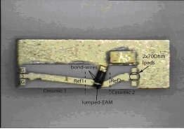
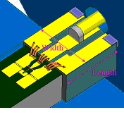
Microphotograph of EML wirebonded onto microstrip lines on ceramic substrate. The EML load is 35 Ohm
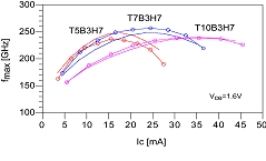
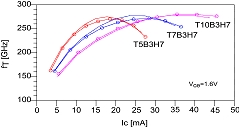
Top figure shows small-signal model fitting to 110 GHz (emitter length: 10µm; Vce=1.6V, Ic=20.5mA).Right figures show the frequency performance versus current for three 0.7µm InP DHBT device geometries (emitter lengths: 5µm, 7µm, 10µm).
EM modelling was used to investigate the performance of packaged photodetector modules for the Rx. Potential bandwidth limiting mechanisms have been identified and suggestions for package optimization have been proposed:
- The transition from 1mm connector to conductor backed CPW was optimized. Guidelines for via placement for low loss, resonance free transmission to 100 GHz was given.
- A full 3D electromagnetic model of a photodetector chip, including transit-time effects was developed. The EM model precisely predicts the measured characteristics of photodiode chips with different p-i-n junctions.
- A new packaged PD module with a thick CPW structure was proposed. The new module exhibits improvement in the measured bandwidth up to 100 GHz and higher relative response over 80 GHz.
A scalable large-signal model for 0.7µm InP DHBT devices has been developed within the GIBON project. The scalable large-signal model includes thermal effects and predicts the RF performance over bias and geometry:
- The large-signal model is based on a modified UCSD HBT model. The scalable model has been made available for both the Agilent ADS and Cadence Spectre simulators with slightly different features.
- In order to arrive at an accurate scalable large-signal model novel parameter extraction strategies for the small-signal model of HBT devices have been developed. In particular the fixed base resistance of sub-micron InP DHBT devices proved to be erroneously extracted using traditional methods. A novel extraction technique for the external base resistance developed within the project made the scalability of the models possible.
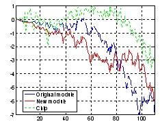
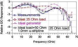
EM-circuit co-simulation of EML u-strip assembly. The wave-like behaviour observed in the measurements is caused by the reflection from the load due to the excessive length of the connecting microstrip line.
EM modelling was also used to investigate the performance of EML for the Tx. Methods were established for the EM simulation of electrical to optical transmission properties of EMLs, both on component level and within high-frequency assemblies:
- Different EML electrode structure options were investigated and suggestions for the best one was given.
- The cause of the unwanted wave-like effect observed in the measurements of the EML in a microstrip assembly was explained using an EM/circuit co-simulation approach.
- The wirebond transition from microstrip lines to EML chip on InP was investigated. A step in ground plane height was shown to introduce little additional losses. Equivalent circuit models for wirebond transitions valid to 100 GHz were developed.